pv magazine: When can we expect the first perovskite modules from serial production with performance warranties of 20 years and longer?

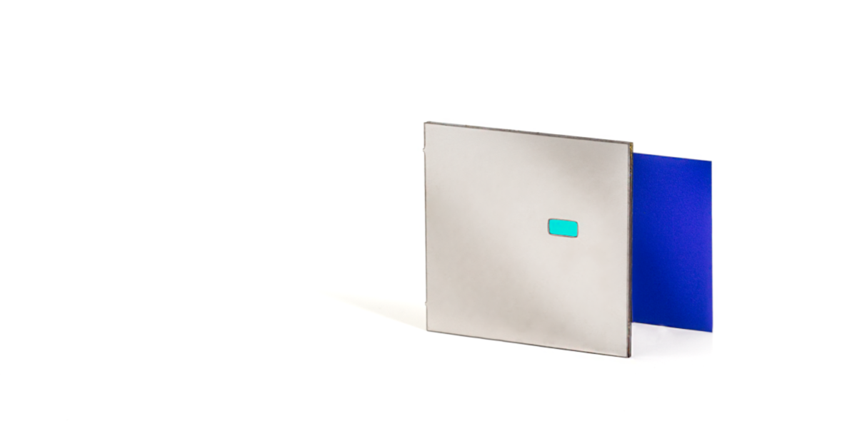
Image: imec
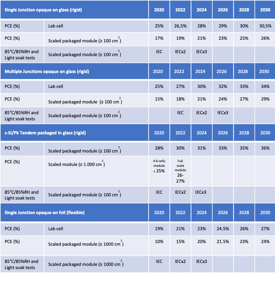
Tom Aernouts: Within two to three years, perovskite-based modules, perovskite-silicon-tandem cells and thin film perovskite cells will be commercially available. Today, tens of companies all over the world are developing manufacturing processes and setting up production capabilities. One of these companies – and one of the forerunners in setting up production facilities – is GCL in China. In the coming two to three years, it is expected that a production capacity of 0.4 to 1.3 GWp will be realized, worldwide. Already by 2020, modules that pass the IEC test will be developed (see figure below). However, the question is if this standard test, which was developed for silicon cells, can also guarantee a 20 year-warranty for perovskite-based cells. It will be key to gain more insight in degradation mechanisms and develop new tests.
For terrestrial applications, will they contain tandem cells with crystalline silicon cells as bases, or will they be a pure thin film perovskite module?
Both options will co-exist and will be used for different applications. Perovskite-silicon-tandem cells will be the perfect option for power generation plants. Despite their higher efficiency compared to silicon cells, they will at first have the ‘disadvantage’ of a higher cost. Indeed, the extra process steps to lay perovskite on top of the silicon is more expensive. However, this cost issue will soon be compensated by a considerably higher conversion efficiency, and the cost will lower once the cells are mass produced. The pure thin film-perovskite modules will be used for integrated applications: in buildings (BIPV) or for infrastructure, for example for cycle lanes or cars. The advantage of the thin film solution is that it can be applied to a flexible substrate, it is light-weight and semi-transparent.
What efficiencies can we expect for c-Si-perovskite tandem cells in R&D and later in serial production?
Perovskite technology is the fastest-advancing solar technology to date with a 3.8% conversion efficiency at its discovery in 2009 to 25.2% in 2019. For tandem cells in particular, an efficiency of 28% has been realized in R&D. This efficiency has the potential to increase to much as 30%, and possibly even higher in the coming years. These results are all still on a rather small area, in the order of 1cm2. In serial production, the tandem module is anticipated to have at least a one or two percentage point higher efficiency on full module size. This allows for a viable market introduction.
Our industry has had bad experiences with the last generation of tandem cells for terrestrial applications – micromorph silicon thin film cells. One of the reasons was the (current) mismatch of the two layers depending on the spectrum of the light, which reduces the specific yield. Is this a severe issue and how can it be tackled?
Also in perovskite-silicon tandem cells, current mismatch will be an issue when operating in outdoor conditions with changing light intensity and spectrum. However, the conversion efficiency when using perovskite as a top layer is much higher as that which has been achieved with micromorph tandem cells.
Current mismatch can be avoided by using 4-terminal instead of 2-terminal concepts. In this case, the tandem sub-cells are electrically isolated from one another and connected in a parallel circuit. 4-terminal-cells are more expensive, because of the extra electrodes and installation costs. Still, when considered on a yearly basis, it may be a more cost-efficient option to use 4-terminal-perovskite-silicon-tandem cells.
2-terminal- and 4-terminal-concepts will coexist and the choice will depend on the application: For a power plant in a desert where light conditions do not vary that much, 2-terminal will be the most cost-effective solution, whereas in most European countries, it will be better to use 4-terminal-tandem cells.
One of the main challenges for perovskites is stability. How much has stability improved in the last three years and what is your prognosis? How was this achieved?
Stability has improved substantially in the last years, to the point that by 2020 the cells will be able to pass the IEC test. First, improvements were made on the material itself. Methylammonium, which appeared to be an unstable compound, was removed from the perovskites. Secondly, the contact layers were adjusted, in order to reduce interactions at the interfaces. It is a fact that the halides iodine and bromine in perovskites easily interact with other materials and this should be avoided. Thirdly, packaging of the perovskite cells protects them against moisture and oxygen, and improves stability. For glass-glass-packaging, expertise from silicon and thin film PV could be used. For flexible pure perovskite modules, an optimized packaging solution will take a bit longer to be developed.
The first perovskites used lead as important component. Has science solved the problem of reducing the lead content? What do you think about the sustainability of perovskite solar cells?
Perovskite technology is considered to be one of the most environmentally-friendly technologies, because of the usage of abundant synthetic components (avoiding mining or heavy purification processes), combined with very low material usage and a low processing temperature. The best efficiencies are still reached with lead-based perovskite cells. Alternatives are being considered, but are still lagging behind. However, the amount of lead used is very low: typical thicknesses of the lead-containing absorber layers are about 0,3µm, resulting in around 1g of lead iodide per m². What is more, even in the case that encapsulated modules are damaged, there is a very low risk of lead leakage. To prevent this from happening, the research community is developing methods to prevent leakage into the environment, by integrating materials that capture the lead or that bind with it to form new compounds that are not water soluble, for example.
Popular content
Lead in c-Si modules
Throughout Q4 2019, pv magazine discussed the use of lead in crystalline solar modules, as part of our global UP sustainability initiative. Check out the October, November and December print magazines to read our UP coverage. To join the conversation, contact up@pv-magazine.com.
How far is the development of production tools for large scale silicon perovskite modules?
Overall, no new production tools need to be developed for silicon perovskite modules. It uses existing industrial processes, such as sputtering and slot-die coating. By making minor adjustments to the tools and processes, the process flow can be set up. This is not a limiting factor for the introduction of this new technology.
What are the production cost projections of silicon perovskite modules? Will they be able to compete with the ever-falling costs for low cost silicon PV, as we have experienced again during the last two years (22 €ct/Watt)?
Because of the extra process steps and material in silicon perovskite modules, they are indeed more costly than pure silicon modules. However, the gain in conversion efficiency outperforms this extra cost. Moreover, manufacturing costs of perovskite PV modules have the potential to be very low. Final costs will depend on materials, stack design and process-selection, as well as on the aimed application and its subsequent market size. Taking all this into account, it is believed that perovskite PV modules can be produced within a cost range of 20 euro-cent/Wp in the coming five to 10 years, and could go down further towards 10 and maybe even to 4 euro-cents/Wp, depending on the learning curve and actual efficiency values on the scaled perovskite PV modules. We can conclude that silicon perovskite modules will definitely be able to compete with current low-cost Si PV technology.
But the 20 euro cent/WP range in five years will not be competitive with the then significant lower cost of crystalline silicon modules. Of course, when you reach 4 cents, this is another story. Do you need subsidies to reach this?
No subsidies are taken into account for these cost targets. Also be sure to make the correct comparison: the 20 cent and down to 4 cent trajectory is for perovskite modules, not for tandems. 20 cents might initially not be competitive with crystalline silicon modules, but it is for sure the cheapest thin film PV then, which also has some market share already now. And you’re comparing with lowest cost crystalline silicon modules typically used for power plant installations. The cost structure for integrated applications, like BIPV, typically allows costs up to five times higher than for power plants. Finally, for tandems, the cost of packaging is already included in crystalline silicon module costs.
What is imec working on concerning the topics discussed?
IMO-IMOMEC, an imec lab at the University of Hasselt, is developing new perovskite materials. Further, imec (in EnergyVille) focuses on upscaling perovskite technology towards industry-relevant 30x30cm modules. More specifically, process steps are tuned, in order to realize high-quality layers, resulting in high efficiencies. The collaboration with Solliance is very important in this context, because of the extensive network with tool suppliers, PV manufacturers and end users.
These upscaled modules can also be tuned in transparency and absorption spectrums such that they can be used for 4-terminal tandems, with crystalline silicon or even other PV technologies. In the case of 2-terminal configurations, a lot of attention needs to be paid to finding the right process conditions to be able to deposit a good-quality perovskite layer on top of the challenging textured surface of the c-Si cell.
What do you think about the chances for European research and production with these new technologies? Will it all go to Asia, as the supply chain for cell production is much better developed there?
As stated in the EPKI Perovskite-PV European White Paper, we believe that this new technology offers unseen opportunities for Europe to gain back control of the PV market. Especially for integrated applications, it will be essential to have production close to the market, because of different regulations and market organization in different countries.
Europe is a forerunner in perovskite research and development. It is important to use this momentum to build a strong industry here. Of course, Asia is top in developing low-cost silicon technology, so it is thinkable that Europe will develop silicon perovskite cells and modules based on cells that are shipped from Asia.
Regarding integrated solutions, I do not understand why it should be easier to be competitive with the large Asian manufacturers, which have significant scale advantages. You also said that GCL is forerunner, so Asian companies do invest in R&D. Why should the customers of integrated solutions opt for more expensive modules made in Europe? Also, is the scale sufficient if one wants to set up production focused on such solutions?
Asian manufacturers have scale advantage for standardized panels, both for crystalline silicon PV and potentially for thin film PV, but once customization – due to application or local regulations – comes in, the cost structure of the installation changes substantially. A solar window or facade element is having an added functionality (generating electricity) on top of its common building element functionality. It will be decisive what the customer wants to pay for this added functionality, potentially induced by local legislation and building rules to integrate it. We’re developing technology that allows for much faster customization as an integrated step in the production process, instead of starting from standard cells or modules and cutting them to the right sizes.
This content is protected by copyright and may not be reused. If you want to cooperate with us and would like to reuse some of our content, please contact: editors@pv-magazine.com.

2 comments
By submitting this form you agree to pv magazine using your data for the purposes of publishing your comment.
Your personal data will only be disclosed or otherwise transmitted to third parties for the purposes of spam filtering or if this is necessary for technical maintenance of the website. Any other transfer to third parties will not take place unless this is justified on the basis of applicable data protection regulations or if pv magazine is legally obliged to do so.
You may revoke this consent at any time with effect for the future, in which case your personal data will be deleted immediately. Otherwise, your data will be deleted if pv magazine has processed your request or the purpose of data storage is fulfilled.
Further information on data privacy can be found in our Data Protection Policy.